
Virtual Event - October 26-29, 2021
Event registration is free courtesy of our sponsors
TestConX has, over the course of its twenty two-year history, established itself as the preeminent event for test consumables, test cell integration, and test operations. The program scope has expanded over these years from packaged semiconductor “final” test and burn-in to encompass all practical aspects of electronics testing including validation, advanced packaging testing, system level test, module test, and beyond to finished product test.
Last year, the 6th annual TestConX China 2020 was held as a virtual live on-line event with excellent average daily attendance of over 800 and peaked with 1188 viewers online at once. (Please see the Post-Event Report for additional details.) We will once again hold TestConX China 2021 as a virtual event using the same online platform. This will provide global attendees with the opportunity to see new locally created and developed content in addition to the best from international presenters.
Don’t miss this opportunity to be part of TestConX as we connect a larger community of test professionals and to participate in this excellent event!
“面向多核算力芯片静默数据损坏的测试和片上容错计算技术”
Abstract (English)
Chip multiprocessors or deep learning processors, provide arrays of processing engines to meet the increasing computing power requirements of various applications. However, silent data corruptions (SDCs) induced by unreliable integrated circuits, impacting the computational integrity of processing engines, have raised increasing attention in industry. For instance, in data centers, the propagation of SDCs can cause data loss and may need months of debugging. This talk will expose the origins of SDCs and emphasize the challenges of sufficient testing of nanotechnology integrated circuits along with opportunities to improve testing. Built-in fault-tolerant computing techniques against SDCs will then be discussed across circuit level, architecture level, and algorithm level, to detect and/or correct the SDCs with low latencies.
摘要 (Chinese)
演讲摘要: 多处理器芯片和深度学习处理芯片通过提供大量处理引擎来满足各类应用日益增长的算力需求,然而,由不可靠的集成电路引发的静默数据损坏(SDC),对计算完整性的影响已经引起工业界的日益重视。例如在数据中心,SDC传播导致的数据丢失可能需要几个月时间去查找问题。讲者将首先探讨SDC产生的原因,阐述对纳米级集成电路测试进行充分测试面临的挑战和提升测试质量的解决方案;然后将介绍应对SDC的片上容错计算技术,涉及在电路级、架构级、算法级等层次如何实现低延时的差错检测和恢复。

MediaTek Inc.
Harry Chen holds the position of IC Testing Scientist at MediaTek Inc. In this role, he investigates advanced design and test methodologies to enhance the performance and quality of leading-edge products. He actively participates in industry forums by publishing papers, giving talks, and serving on program committees. He also supports academic research projects and trains student interns. He is the section leader for System-Level Test (SLT) in the IEEE Heterogeneous Integration Roadmap (HIR) Test Chapter. With more than 30 years in the semiconductor industry, Harry has held previous technical positions at Cadence Design Automation and Analog Devices in the USA. His EE degrees were obtained from MIT and Stanford University.
“利用大数据系统的AI技术优化测试成本”
Abstract - Biography (English)
With the rapid development of the semiconductor industry, the volume of data generated during the mass production process has increased dramatically, providing a rich source of information for semiconductor testing. This paper proposes an analytical method based on Gubo OneData big data system to mine and analyze the vast amount of semiconductor testing data to discover potential correlations between different testing phases. By constructing advanced data mining algorithms, this study is able to identify key test items affecting the performance of semiconductor products and further evaluate the interrelationships among these test items. The results show that by optimizing the testing process and eliminating redundant or inefficient test items, production costs can be significantly reduced while ensuring product quality. This paper details the entire process of data collection, preprocessing, feature selection, model construction, and validation, and presents practical application cases, proving the effectiveness and feasibility of the method in actual production environments. Ultimately, this study provides a new cost optimization strategy for the semiconductor industry, which helps to promote technological progress and economic benefits in the industry.
Keywords: Semiconductor Testing; Big Data Analysis; Data Mining; Cost Optimization; Correlation Analysis
Lisi Ma as one of the core team members of Gubo Technologies, Lisi Ma is currently in charge of the Product Management and Design Team. His expertise and domain of responsibilities extend to areas including testing and automation, data analysis, and the product definition of enterprise-level R&D product management platforms. He leads the team in conducting multiple in-depth collaborations with top-tier design companies in China.
摘要 - 简介 (Chinese)
随着半导体行业的快速发展,大规模生产过程中产生的数据量急剧增加,为半导体测试提供了丰富的信息资源。本文提出了一种基于孤波OneData大数据系统的分析方法,旨在通过挖掘和分析海量半导体测试数据,发现不同测试阶段之间的潜在相关性。通过构建先进的数据挖掘算法,本研究能够识别出影响半导体产品性能的关键测试项目,并进一步评估这些测试项目之间的相互关系。研究结果表明,通过优化测试流程,剔除冗余或低效的测试项目,可以显著降低生产成本,同时保证产品质量。本论文详细介绍了数据收集、预处理、特征选择、模型构建和验证的全过程,并展示了实际应用案例,证明了该方法在实际生产环境中的有效性和可行性。最终,本研究为半导体行业提供了一种新的成本优化策略,有助于推动行业的技术进步和经济效益的提升。
关键词:半导体测试;大数据分析;数据挖掘;成本优化;相关性分析
马力斯作为上海孤波科技有限公司的核心团队成员之一,目前负责产品管理与设计团队。他的专业领域包括测试与自动化、数据分析以及企业级研发产品管理平台的产品定义。他带领团队与国内一线设计公司进行多个深度合作。
“生物微机电芯片湿测试平台的开发与验证”
Abstract - Biography (English)
According to the Yole 2023 report, the production value of silicon-based biomedical chips is expected to reach US$900 million by 2027. After the outbreak of COVID-19, many medical institutions found that traditional PCR testing was too slow. The need for fast detection led many companies to invest in the development of new types of BioMEMS. MEMS technology can reduce the size of BioMEMS chips and integrate microfluidic systems. The microstructure on BioMEMS can effectively reduce the usage of reagents. The testing requires only a small amount of sample, reagent, and testing time to obtain results. On the other hand, even with the strong performance of BioMEMS, due to the lack of mature mass production testing technologies, the low coverage rate of mass production testing causes the BioMEMS production capacity to be unable to increase.
This study developed a wet testing platform for BioMEMS chips and achieved stable and highly reproducible measurement results. BioMEMS chips require additional wet testing to verify product yield. In the wet testing process, the test solution is dispensed onto the sensing area of the chip test key, the Kelvin pin makes contact with the pad, and then electrical testing can commence. In addition, due to the restriction of the structure and size of the BioMEMS chip, the volume of the solution to be tested must be controlled within a micro volume of 1 μl. Based on the above situations, this study developed the wet testing platform according to the droplet testing method used in the past. The wet testing platform integrates and optimizes the probe station, semiconductor analyzer, and microfluidic control system. The testing method also verified the influencing factors such as solution concentration, different solutions, cleaning methods, testing time, and needle force, and used the experimental results to improve the testing process. Additionally, this study developed a water-retaining shield method for long-term testing. The shield prevents test sample evaporation and environmental effects. In long-term testing, the shield prolonged the testing time and stabilized the measurement data. This testing platform and process were also verified with the BioMEMS chips, and the measurement data of electrical properties not only showed accuracy but also reproducibility. In summary, the developed wet testing platform can provide reliable electrical measurement capability and has the potential to be developed into a semi-automatic and fully automatic testing platform. The technology is expected to be applied in the field of contract manufacturing testing in the future.
Po-Ting Lai joined King Yuan Electronics in 2018 and is currently a staff engineer in the Advanced Test Development & Application division.
Over the past seven years, his work specifically focusing on developing mass production testing technologies for bioMEMS and microfluidic chips.
In recent years, his team has presented their research findings at the 2020 ITC-Asia, 2023 ITC-Asia, and 2024 ICSS conferences, and has been awarded several invention patents.
摘要 - 简介 (Chinese)
生物微机电(BioMEMS)在生医芯片中是个发展迅速的领域,根据2023的产业报告,生医芯片的产值在2027预计将达到9亿美元。此外在新冠疫情爆发后,让医学单位发现传统PCR的速度太慢,故许多企业与实验室皆投入新型生物微机电的开发。微机电技术可以减小芯片的尺寸,并集成微流控技术。芯片上的微结构可以有效减少试剂的用量,检测只需要少量的样品、试剂及测试时间便能够得到结果。另一方面尽管生物微机电芯片具有出色的性能,但由于缺乏成熟的大规模量产测试技术,导致量产测试覆盖率低迷,使得终端产能无法提升。
此次的研究,我们根据客户的生物微机电芯片开发了一个手动测试平台,并实现了稳定且高度可重复的量测结果。许多生物微机电芯片需要额外的湿测试(wet testing)来验证产品的良率。在湿测试过程中,测试溶液会滴到芯片测试键(chip test key)的感测区域,并在测试键上的芯片座(chip pad)扎针(probing)后才能进行电性测试。由于此芯片的结构尺寸反应区域与芯片座距离太短,使待测液的体积受限,必须控制在1微升以内的微体积。基于上述状况,此研究根据过去的滴珠测试方法开发了具自动化潜力的湿测试平台。此湿测试平台整合与优化了探针台、半导体分析仪、微流体控制系统。测试方法同时对各待测液浓度、种类、待测液清洁方法、测试时间、下针力道等影响因子进行验证,并利用实验结果完成测试流程的改善。此外用于长期量测,本研究开发了一种挡水墙屏蔽方法。这种屏蔽能防止测试样品受到环境影响而蒸发。在长期测试中,屏蔽能延长测试时间并使测量数据更加稳定。该测试平台和流程也在客户的生物微机电芯片上进行了验证,电性测量数据不仅显示了其准确性,还展示了其可重复性,其成果也受到客户的肯定。总而言之,开发的湿测试平台具备可靠的电性测量能力,并有潜力发展成为半自动和全自动测试平台。预计该技术未来可应用于代工量产测试领域。
賴柏廷于2018加入京元电子,现在于尖端测试技术开发处担任资深工程师,
这七年主要专注于生物微機電与微流道芯片,目标是开发相关产品的量产测试技术,
其团队近年的研究成果已成功于2020 ITC-Asia、2023 ITC-Asia、2024 ICSS进行发表,并获得数个专利
“台式电脑和边缘设备浸没式冷却技术小型化的参数研究 ”
Abstract - Biography (English)
The compute power of stationary Small Form Factor (SFF) systems, such as desktops or Internet-of-Things (IOT) edge devices, are often thermally limited by the constrained space which makes it a challenge to support the Processor Base Power (also known as Thermal Design Power, i.e. TDP). While customers want to take full advantage of Intel processors with turbo performance, it is even more incredibly challenging to meet the additional thermal requirements by using traditional air-cooling technology in SFF systems. What adds to the pain point is that the system often operates in high operating ambient temperature (in the range of 50-60°C) for IOT applications.
Liquid immersion cooling is one of the most recent innovative technologies in which electronic systems are submerged in a non-conductive liquid bath to allow much more effective cooling. While it is commonly deployed for heat-intensive large-scale servers, we are taking proactive measures to perform sensitivity study to miniaturize immersion cooling to a desktop-tower-size system. The goal of this study is to achieve the smallest possible tower size with the targeted power dissipation. We will demonstrate the proof-of-concept (POC) system equipped with single phase liquid immersion cooling and measure the temperature on the dummy heater units, which mimic an Intel processor and a discrete graphic component. A series of parametric studies were performed to optimize the system in order to achieve the targeted power dissipation.
This paper presents the optimization approach and the components that were changed to arrive at the final POC. The POC that we present in this study measures 160mm (W) x 405mm (H) x 300mm (L) with volumetric size approximately 19.4L. The combined total power dissipation from the heaters is 650W. This POC is the smallest form factor that we can achieve based on the design requirements we have set forth. We believe this concept study with immersion liquid cooling can be scaled to Intel high performance processors with a discrete graphics card which brings the next level of user experience in the desktop, IOT, and workstation user space.
Khai Ern is currently the Platform Architect in the CCG-Malaysia Client Customer Engineering team at Intel. His experience spans multiple computing segments, from tablets and laptops to desktop PCs. He was part of the pioneering team that created the Intel Compute Stick and the first Intel Dual Screen Device Proof-of-Concept prototype, which eventually became successful customer products. His current focus is on defining the system architecture for the next generation of laptop systems, where he collaborates with PC industry players to advance the compute user experience. He is an active technical paper writer with over 30 publications and presentations at technical conferences, where he has received multiple best paper awards.
Johnson Tao is a senior system architect engineer from Client Computing Group(CCG) based in Shanghai PRC.
He is responsible for the intel platform customer enabling and innovation for customer feature landing. Johnson joined Intel in 2011. He received his EE bachelor degree from Nanjing university China, master Degree of EEE from Nanyang technological university Singapore
摘要 - 简介 (Chinese)
固定式小型机箱(SFF)系统,如台式电脑或物联网(IOT)边缘设备的计算能力,往往因空间受限而在热量上达到极限,这使得支持处理器基础功率(也称为热设计功率,即TDP)成为一项挑战。尽管客户希望充分利用英特尔处理器的高频性能,但在SFF系统中使用传统的空气冷却技术来满足额外的热量要求则更加具有挑战性。痛点在于,系统常常在高环境温度下运行(物联网应用的温度范围在50-60°C),这进一步增加了难度。
液体浸没冷却是一种最新的创新技术,电子系统被浸入非导电液体中,以实现更有效的冷却。虽然这种技术通常用于热量密集的大型服务器,但我们采取积极措施,进行敏感性研究,以将浸没冷却技术缩小到台式机塔式系统。这项研究的目标是实现尽可能小的塔式机箱尺寸,同时达到目标的功率耗散。我们将展示配备液体浸没冷却的概念验证(POC)系统,并测量模拟英特尔处理器和独立图形处理器的负载单元的温度。我们进行了一系列参数研究,以优化系统,达到目标的功率。
本文介绍了优化方法和为达到最终POC而更改的组件。我们在这项研究中展示的POC尺寸为160mm(宽)x 405mm(高)x 300mm(长),体积大约为19.4L。来自加热器的总功率耗散为650W。这个POC是我们基于我们设定的设计要求所能实现的最小形式机箱。我们相信,这项带有浸没液体冷却的概念研究可以扩展到英特尔高性能处理器和独立显卡,为台式机、IOT和工作站用户带来下一级别的用户体验。
陶剑诚,英特尔亚太研发有限公司(上海)系统设计架构师。2011年加入英特尔计算与客户集团,主要负责大中国区计算机客户支持,研发与创新功能落地。陶剑诚本科毕业于南京大学,研究生毕业于新加坡南洋理工大学。
“通过自动化和热管理中的高级仿真优化半导体测试”
Abstract - Biography (English)
In the dynamic and competitive semiconductor industry, optimizing test equipment throughput and managing thermal performance are essential for efficiency and productivity. However, predicting automation throughput and thermal behavior remains a complex task. This presentation explores how simulation can transform the prediction of both automation throughput and thermal performance for semiconductor test equipment.
By using simulation, we can create virtual models that replicate real-world semiconductor testing conditions. This discussion will cover how simulation allows us to model the intricate interactions between equipment modules, processes, resources, and thermal dynamics, enabling accurate forecasts of both performance and thermal characteristics. We will also delve into the benefits of using simulation, such as optimizing equipment utilization and power loads. By modeling the automation process flow, potential bottlenecks and inefficiencies can be identified, allowing for proactive adjustments and continuous improvement.
This presentation will provide detailed examples of how thermal simulation can be leveraged to enhance the design of thermal solutions, effectively addressing challenging thermal issues in semiconductor testing. We will explore specific cases where thermal simulation has been used to identify and mitigate thermal challenges during testing, such as thermal hotspots and thermal gradients.
Key Takeaways:
- Understanding the role of simulation in predicting automation throughput and thermal performance for semiconductor test equipment.
- Examples of simulation optimizing equipment utilization and predicting thermal behavior of a DUT.
- Benefits of using simulation, including optimized resource utilization, reduced cycle times, improved equipment efficiency, and thermal load management.
- The role of simulation in scenario analysis and data-driven decision-making for continuous improvement.
- Strategies for leveraging simulation to drive efficiency and gain a competitive edge in the semiconductor industry.
Sid Chan obtained his MSc of Mechanical Engineering from the Sheffield Hallam University, UK.
Sid Chan joined AEM Singapore in 2010. In his 13 years with AEM, Sid Chan has been playing the role of solution architect for multiple development projects of semiconductor test equipment for FT, SLT, and Burn-in. Most of these projects are now in mass production and deployed to the world’s top semiconductor company.Sid Chan currently leads the product development team in AEM Singapore to develop new technology for semiconductor test handling. The focus area includes automation, thermal control solution, and tester integration.
摘要 - 简介 (Chinese)
在充满活力和竞争的半导体行业中,优化测试设备吞吐量和管理热性能对于效率和生产力至关重要。然而,预测自动化吞吐量和热管理仍然是一项复杂的任务。本演示探讨了仿真如何改变半导体测试设备的自动化吞吐量和热性能预测。
通过使用仿真,我们可以创建真实半导体测试条件的虚拟模型。本次讨论将介绍仿真如何让我们对设备模块、流程、资源和热动力学之间的复杂交互进行建模,从而准确预测性能和热特性。我们还将深入研究使用仿真的好处,例如优化设备利用率和电力负载。通过对自动化流程进行建模,可以识别潜在的瓶颈和低效率,从而允许主动调整和持续改进。
本演示将提供详细的示例,说明如何利用热仿真来增强热解决方案的设计,从而有效解决半导体测试中具有挑战性的热量问题。我们将探讨使用热量仿真来识别和缓解测试过程中的热挑战的具体案例,例如热点和热梯度。
关键要点:
- 了解仿真在预测半导体测试设备的自动化吞吐量和热性能方面的作用。
- 模拟优化设备利用率和预测 DUT 的热行为的示例。
- 使用仿真的好处,包括优化资源利用率、缩短周期时间、提高设备效率和热负荷管理。
- 模拟在情景分析和数据驱动决策中的作用,以实现持续改进。
- 利用仿真提高效率并在半导体行业获得竞争优势的策略。
Sid Chan 毕业于英国谢菲尔德哈勒姆大学,并获颁机械工程硕士学位。
Sid Chan 于 2010 年加入 AEM 新加坡。在 AEM 工作的 13 年中,Sid Chan 一直担任 FT、SLT 和老化半导体测试设备开发项目的解决方案架构师。这些项目中的大多数现在都已投入量产,并已部署到世界顶级半导体公司。
Sid Chan 主要领导 AEM 新加坡的产品开发团队开发用于半导体测试处理的新技术。重点领域包括自动化、热控制解决方案和测试仪集成。
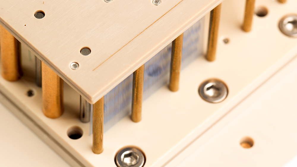
“弹簧探针的耐电流能力评估”
Abstract - Biography (English)
The spring probe contact Current Carrying Capacity(CCC) is critical for a connector or IC test socket, it is one of key factors to assess if the spring probe contact can work for the application. The maximum continuous current rating of a high current spring probe is determined by its design, size, material, construction, etc. In many cases at a spring probe development early development stage, the rated CCC are just a rule of thumb based on engineers’ experience. The paper will introduce a different method to predict the spring probe current carrying capacity at early development stage.
Frank Liu graduated from Shandong University of Science and Technology in 2001, majoring in Mechanical design and manufacturing. He studied for his MBA in Tongji University in 2018. Frank Liu started working in Smiths Interconnect Suzhou in 2007, and now he is Engineering Manager for Semi test product development.
摘要 - 简介 (Chinese)
弹簧探针的耐电流能力对连接器和芯片测试座来讲至关重要,它用来评估弹簧探针是否满足产品应用的一个重要指标。弹簧探针的最大耐流能力通常由产品的设计、大小、材料、结构等决定。通常在弹簧探针的开发初期,弹簧探针的耐流能力往往是工程师通过经验法则来预测。这篇文章介绍了另外一种探针研发初期,预测弹簧探针耐流能力的方法。>/p>
刘德先,2001年毕业于山东科技大学,所学专业是机械制造工艺与设备专业。2018年参加同济大学的工商管理硕士(MBA)的学习。2007年起,刘德先就职于史密斯英特康苏州,目前作为工程研发经理负责半导体测试新产品开发。

VLSIresearch
Lin is a Principal Analyst of VLSI Research Europe. She received the Doctoral Degree in Engineering from University of Cambridge in 2017. Lin has published more than 20 academic papers as the first author or co-author in the IEEE Transactions, SUST, Journal of Physics D etc.
Lin started to join VLSI Research Europe from February 2017, focusing on the technical and marketing research and analysis related to semiconductor test consumables. She has been responsible for expanding VLSI Research Europe's coverage of the test consumables market, which now includes detailed breakouts of the non-memory market and market data on materials and components.
“新兴需求下射频测试技术与高速数字信号测试技术的融合趋势”
Abstract - Biography (English)
With the rise of the RF sampling ADC/DAC, PCIe 5/6, 1.6/3.2T Ethernet, and other products with high-speed interfaces, how to effectively test these products has become a new hot issue. As these DUTs have the characteristics of both high-frequency and high-speed, it is worthwhile to explore how to better characterize their performance and reliability in real-world applications. On the other hand, testers themselves are facing the opportunity to completely update their architectures by adopting, for example, RF digitization, which allows them to gain enhanced or even completely new test capabilities by taking advantage of RF/high-speed digital hybrid technologies. This paper attempts to discuss these issues and to share with you some of the latest advances in this domain from MET.
Daniel Xiao, PhD. Chairman of Suzhou MET Technology Co., Ltd. Graduated from Peking University with a major in Signal and Information Systems. He is the Chairman of Suzhou MET Technology Co., Ltd. He has long been dedicated to the design and development of a new generation of highly reliable RF sampling transceiver module, leading his team to achieve the productization of high anti-interference RF sampling transceiver technology comparable to heterodyne architecture indicators.
MET, the company he founded, is a technology innovation company committed to the research and development of testers for RF/microwave and high-speed interface chips/module. MET possesses original breakthroughs and deep accumulation in supporting fields such as digital RF transceiver modules, measurement algorithms and models, and industrial test software.
摘要 - 简介 (Chinese)
随着射频采样ADC/DAC、PCIe 5/6总线产品、1.6/3.2T以太网等具备高速接口的产品的兴起,如何对这些产品进行有效的测试也成为一个新的热点问题。这类被测件兼具高频器件和高速器件的特征,从何种角度可以更好地表征他们在真实应用场景下的性能和可靠性值得被认真探讨。另一方面,测试机本身也面临着利用诸如硅基射频数字化技术来全面更新自身架构的机遇,这使得测试机自身通过发挥射频/高速数字混合技术的优点而获得了更强的、甚至全新的测试能力。本文试图对上述问题进行抛砖引玉式地探讨,与诸位专家分享美星科技在这个领域的一些最新的进展。
肖如吾博士,苏州美星科技有限公司董事长。毕业于北京大学,专业为信号与信息系统。他长期致力于新一代高可靠性射频采样收发模块的设计与开发,带领团队实现了与外差架构指标相当的高抗扰性射频采样收发技术的产品化。
美星科技,他创办的公司,是一家致力于射频/微波和高速接口芯片/模块测试设备研发的科技创新公司。美星科技在数字射频收发模块、测量算法与模型、工业测试软件等支撑领域具备原创突破和深厚积累。
“电池单元和电动车连接器应用的测试探针和接触器:挑战与创新解决方案”
Abstract - Biography (English)
In our paper, we present state-of-the-art and novel probe designs for battery cell and EV-connector contacting applications. The purpose of these test products is to establish a temporary interconnect with the battery or a connector on an inverter for testing the unit (end of line test). Among the tests, we will cover topics such as charge/discharge, OCV, weld joint test, and electrochemical impedance spectroscopy. Besides testing, we will also focus on the topic of battery cell formation and probe/contact choice for this application. The challenge is that the parts need to remain in the formation rack for a very long time (several years), and the formation process takes quite a bit of time as well. This has an impact on tip wear and probe life. We’ll demonstrate methods that can be implemented to ensure the parts can be cleaned with “in situ” methods without the need to remove them from the rack. Lastly, we’ll present some new unique challenges, such as the need for an extremely increased current rating. Since this can negatively affect probe performance, interesting novel concepts are presented to cool down the probe in a tester or formation rack.
Matthias Zapatka is the co-founder of INGUN USA, the North American subsidiary of the INGUN group. He has over 16 years of experience in the field of PCBA testing, specializing in spring-contacts, probes, and test fixtures. Matthias’ academic background is in RF & Wireless technologies. He graduated with honors from Konstanz University of Applied Sciences in Germany in 2008. He is a regular speaker at industry-related events and is IPC certified as an “Interconnect Specialist.” Matthias resides in the western part of the United States.
Fred Li is Working in Ingun China, Battery unit member of Ingun group. More than 10 years experience in automation and precision manufacturing. Now focus on the battery and its related industries.
摘要 - 简介 (Chinese)
在我们的论文中,我们展示了用于电池单元和电动车连接器接触应用的最先进和新颖的探针设计。这些测试产品的目的是在电池或逆变器上的连接器上建立临时互连,以便对单元进行测试(生产线末端测试)。在测试中,我们将涉及充电/放电、开路电压(OCV)、焊接接头测试和电化学阻抗谱等主题。除了测试外,我们还将关注电池单元的成形以及该应用中的探针/接触选择。挑战在于这些部件需要在成形架上保持很长时间(数年),而成形过程也需要相当长的时间。这会影响探针的磨损和使用寿命。我们将演示可以实施的方法,以确保这些部件可以通过“原位”方法进行清洁,而无需将其从架子上取下。最后,我们将介绍一些新的独特挑战,例如对极高电流等级的需求。由于这可能对探针性能产生负面影响,我们提出了一些有趣的新颖概念,用于在测试器或成形架中冷却探针。
Matthias Zapatka 是INGUN USA的联合创始人,该公司是INGUN集团在北美的子公司。他在PCBA测试领域拥有超过16年的经验,专注于弹簧接触器、探针和测试夹具。Matthias的学术背景为射频与无线技术,他于2008年以优异的成绩毕业于德国康斯坦茨应用科技大学。他经常在行业相关活动中演讲,并且是IPC认证的“互连专家”。Matthias居住在美国西部。
Fred Li在INGUN中国工作,是INGUN集团电池单元的成员。他拥有超过10年的自动化和精密制造经验,目前专注于电池及其相关行业。
“电池管理系统的自动测试设备:挑战和解决方案””
Abstract - Biography (English)
This presentation discusses the challenges of automated test equipment (ATE) for testing battery management systems (BMS) in electric vehicles (EV) and introduces novel system-architectural solutions based on highly integrated system-on-a-chip (SOC) parametric measurement units (PMUs).
BMS measure temperature, voltage, and current in the battery-pack and balance battery cell charge. However, ATE for testing BMS in EVs has several challenges: Since a BMS device-under-test (DUT) may support a battery module with a series-connected stack of 16 or more Lithium-Ion cells, traditional ATE based on discrete devices has low density since it requires a high number of voltage and/or current source stimuli to emulate individual cell outputs. Second, since the DUT needs to be tested to microVolt (uV) and microAmpere (uA) accuracy, the ATE needs low-noise, precision voltage, and current sources which increase implementation complexity, size, and cost of discrete solutions. Moreover, the test stimuli to the BMS-DUT may require 100’s of Volts common-mode voltage relative to the channel differential voltage. Finally, since discrete-device-based ATE is not readily scalable, testing various BMS and battery-module configurations requires custom designs which take longer to build.
As a solution to the above challenges, this work first presents a series-connected stack of floating-ground PMUs which connect to the DUT and test if its cell-voltage (CV) and cell-balance (CB) terminal characteristics meet their specifications. The floating-ground-based topology meets both the high common-mode and the uV/uA precision requirements noted above. Each PMU has an isolated power supply for galvanic isolation from the system input power supply. In this configuration, digital-to-analog converters (DACs) integrated in each PMU drive the DUT CV and CB terminals in force-voltage (FV) or force-current (FI) mode and validate the DUT battery-cell measurement, input-current, and CB switch-transistor on-resistance capabilities from the DUT measure-current (MI) and measure-voltage (MV) responses. Each PMU FV or FI stimulus can be independently programmed by ATE software, thereby enabling test coverage of any battery cell condition. Following the above discussion, a second topology is presented which extends the testable DUT voltage range up to its absolute maximum rating by connecting each PMU in series with a high-voltage common-mode (CM), efficient switching-mode-power-supply (SMPS). The system is reconfigurable between the first high-precision and the second extended-voltage-range topologies using switching matrices. These switching matrices may be discrete to support more flexibility or integrated with the PMU, e.g., as co-packaged Micro-Electromechanical Systems (MEMS) switches. At the circuit level, integrated clamps in the PMU limit the voltage and current across the DUT. Additionally, each PMU has alarm features which detect temperature, voltage, current, and force/sense Kelvin faults.
BMS future trends include support for higher-voltage battery-packs, higher precision, various pack topologies as well as several new functions including active management and active cell balance. The presented architecture is scalable and readily addresses these trends because of design choices such as the integrated PMU SOC, series-connected PMUs / stacking of PMUs on CM power supply, and reconfigurability between the two topologies via the MEMS switching-matrix.
Sandeep D’Souza is a Principal Engineer with ElevATE Semiconductor working on integrated circuit and system design for Automated Test Equipment (ATE) applications. He has 24 years’ experience in the semiconductor industry on ATE, Semiconductor Device Modeling, Analog, Mixed-Signal and RF IC design, and systems design for Ultrasonic Sensor, Haptics, Audio and Touch-Controller applications. Prior to ElevATE, he was with Qualcomm, Semtech (Jariet), Skyworks and Conexant. He has 8 publications and 40+ issued / pending patents. He received his Bachelor, Master and PhD degrees all in Electrical Engineering from IIT Bombay, Purdue University and UCLA respectively.
摘要 - 简介 (Chinese)
本演讲讨论了用于测试电动汽车 (EV) 中的电池管理系统 (BMS) 的自动测试设备 (ATE) 所面临的挑战,并介绍了基于高度集成的片上系统 (SOC) 参数测量单元 (PMU) 的新型系统架构解决方案。
BMS 测量电池组中的温度、电压和电流并平衡电池单元电量。然而,用于测试电动汽车中 BMS 的 ATE 面临多项挑战:由于 BMS 被测设备 (DUT) 可能支持具有 16 个或更多锂离子电池串联堆栈的电池模块,因此基于分立设备的传统 ATE 密度较低,因为它需要大量电压和/或电流源刺激来模拟单个电池输出。 其次,由于 DUT 需要以微伏 (µV) 和微安 (µA) 的精度进行测试,因此 ATE 需要低噪声、精密电压和电流源,这会增加分立解决方案的实施复杂性、尺寸和成本。此外,对 BMS-DUT 的测试刺激可能需要相对于通道差分电压的数百伏共模电压。最后,由于基于分立器件的 ATE 不易扩展,因此测试各种 BMS 和电池模块配置需要定制设计,而这需要更长的时间来构建。
作为上述挑战的解决方案,这项工作首先提出了一个串联的浮地 PMU 堆栈,它们连接到 DUT 并测试其电池电压 (CV) 和电池平衡 (CB) 端子特性是否符合其规格。基于浮地的拓扑结构既满足上述高共模要求,也满足 µV/µA 精度要求。每个 PMU 都有一个隔离电源,用于与系统输入电源进行电气隔离。 在这种配置中,每个 PMU 中集成的数模转换器 (DAC) 以驱动电压 (FV) 或驱动电流 (FI) 模式驱动 DUT CV 和 CB 端子,并根据 DUT 测量电流 (MI) 和测量电压 (MV) 响应验证 DUT 电池单元测量、输入电流和 CB 开关晶体管导通电阻能力。每个 PMU FV 或 FI 刺激都可以由 ATE 软件独立编程,从而实现对任何电池单元条件的测试覆盖。根据上述讨论,提出了第二种拓扑,通过将每个 PMU 与高压共模 (CM)、高效开关模式电源 (SMPS) 串联,将可测试的 DUT 电压范围扩展到其绝对最大额定值。该系统可以使用开关矩阵在第一种高精度拓扑和第二种扩展电压范围拓扑之间重新配置。 这些开关矩阵可以是离散的以支持更大的灵活性,也可以与 PMU 集成,例如作为共同封装的微机电系统 (MEMS) 开关。在电路级,PMU 中的集成夹具限制了 DUT 上的电压和电流。此外,每个 PMU 都具有报警功能,可检测温度、电压、电流和强制/感测开尔文故障。
BMS 的未来趋势包括支持更高电压的电池组、更高的精度、各种电池组拓扑以及包括主动管理和主动电池平衡在内的多项新功能。由于设计选择,例如集成的 PMU SOC、串联 PMU/CM 电源上的 PMU 堆叠以及通过 MEMS 开关矩阵在两种拓扑之间进行重新配置,所提出的架构是可扩展的并且可以轻松应对这些趋势.
Sandeep D’Souza 是 ElevATE Semiconductor 的首席工程师,致力于自动测试设备 (ATE) 应用的集成电路和系统设计。 他在半导体行业拥有 24 年从业经验,擅长 ATE、半导体器件建模、模拟、混合信号和 RF IC 设计,以及超声波传感器、触觉、音频和触摸控制器应用的系统设计。在加入 ElevATE 之前,他曾就职于 Qualcomm、Semtech (Jariet)、Skyworks 和 Conexant。他发表了 8 篇论文,拥有 40 多项已发布/待批专利。他分别在孟买印度理工学院、普渡大学和加州大学洛杉矶分校获得了电气工程学士、硕士和博士学位.
“大规模芯片ATE量产测试板诊断方案 ”
Abstract - Biography (English)
Diagnosis Plan for ATE Production Test Board of Large-Scale Chip
With increasing chip integration as well as ATE test sites, the complexity of test boards also increased exponentially, resulting in some of the test boards having more that tens of thousands of component counts. This increases the difficulties in the both debugging and maintaining the test boards
The flying probe test and simple electrical test from manufacturers are no longer sufficient to find the faults of test board. Three main challenges faced are as follows:
- Unable to confirm in advance whether the test board is operational before retest.
- Unable to quickly ascertain if the boards are abnormal during mass production.
- Unable to quickly locate failed components when encountering test board problems resulting in lower productivity.
This material provides a systematic solution which can solve the above problems quickly through:
- Hardware: Using one-time investment low-cost customized dummy devices that can be utilized throughout the product life-cycle to cover all important components on the ATE test boards without the need for LB design changes or additional devices.
- Software: Code Library is made to simplify development efforts and achieve a friendly user interface. At the same time, the fault component reference number can be printed out through the datalog which is very convenient towards maintenance.
Results: Generally, there are more than 15000 mounted components on test board for AP chip, this method of test can cover 90% of them, and can successfully identified many functionally defective parts through the diagnosis plan.
Jiang Lei, joined UNISOC Co., Ltd in 2014. He serves as a Senior Staff Test Engineer in the SEG (System Engineer Group). With over 10 years of experience in ATE hardware design and SOC/PMIC/RF debugging, he is highly experienced in the design and simulation of high-speed and RF signals. Additionally, he holds 8 patents related to ATE.
摘要 - 简介 (Chinese)
大规模芯片ATE量产测试板诊断方案
随着芯片的复杂度增加和ATE测试的同测数增加,ATE测试板的复杂度也会指数级增加,部分测试板上的器件总数已经超过数万个,导致ATE测试板前期的验收调试及后续的量产维护都非常困难,测试板厂商能提供的飞针测试及简单的电气测试已经不够;
当前的困难主要是以下三点:
- 芯片回片前无法确认测试板是否能正常使用
- 量产时遇到异常无法快速排查是不是硬件导致的问题
- 量产时遇到硬件问题无法快速定位失效器件,影响产出
本次材料从硬件/软件两个维度提供了一种系统性的解决方案,可以快速解决以上问题:
- 硬件:在不改变现有测试板设计,不增加复杂度的情况下,用少量成本定制一套PCB,覆盖测试板上所有重要器件的测试路径,只需一次性投入,整个产品生命周期内都可以使用
- 软件:将Code Library化,简化开发工作,实现友好的用户接口,同时可以通过Log打印出Fail器件位号,方便工厂维护;
- 使用效果:通常AP芯片的测试载板上器件数量会超过15000个,使用本方案后器件覆盖率可超过90%,我们通过本方案排查到了不少异常的器件
雷江,2014年加入紫光展锐有限公司,担任测试工程系统架构部高级主任测试工程师。他有超过10年的ATE硬件设计经验和SOC/PMIC/RF的调试经验,并在高速信号和射频信号的设计/仿真方面有丰富的项目经验积累。此外,他还拥有8个与ATE硬件相关的专利。
For any questions about the event or sponsorship contact us at [javascript protected email address].
Program subject to change without notice
Event registration is free courtesy of our sponsors
Honored Sponsor

JDT Technology's focus in the vertical field of semiconductor and electronic product testing & precision manufacturing, and dedicate ourselves to be an “Intelligent Automation Integrated Solution Provider”. Our main business includes: Probe materials, ICT / FCT test fixtures, Automated Testing Equipment & Precision Machining.
Distinguished Sponsors

Smiths Interconnect is a leading provider of innovative solutions for critical semiconductor test applications. Smiths Interconnect’s test sockets and probe card solutions offer superior quality and reliability, providing customers with a competitive advantage. Our best-in-class engineering, development and technical expertise ensure support of automated, system level and development test platforms for area array, peripheral, wafer level and Package on Package (PoP) devices as well as high performance spring probe technology and cable assemblies. Our extensive product portfolio accommodates devices with finest micro pitches as well as those with very high bandwidth requirements. Off-the -shelf and custom products are proven to deliver the best solution for the customer’s specific needs.
For more information, please visit www.smithsinterconnect.cn


"Toward the Company Creating the Future Value of Technology"
As a Technology and Science Enabler in the field of Semiconductor Test and Display Test, TSE has developed the innovative technologies needed by its customers and has engaged in continuous research and productivity improvement activities. Founded in 1994, it has engaged as a leader in interface systems for Semiconductor Test.
Exhibitor Sponsors
Advantest is the leading manufacturer of automatic test and measurement equipment used in the design and production of semiconductors for applications including 5G communications, the Internet of Things (IoT), autonomous vehicles, artificial intelligence (AI), machine learning, smart medical devices and more. Its leading-edge systems and products are integrated into the most advanced semiconductor production lines in the world. The company also conducts R&D to address emerging testing challenges, produces multi-vision metrology scanning electron microscopes essential to photomask manufacturing, and offers groundbreaking 3D imaging and analysis tools. Founded in Tokyo in 1954, Advantest is a global company with facilities around the world and an international commitment to sustainable practices and social responsibility.